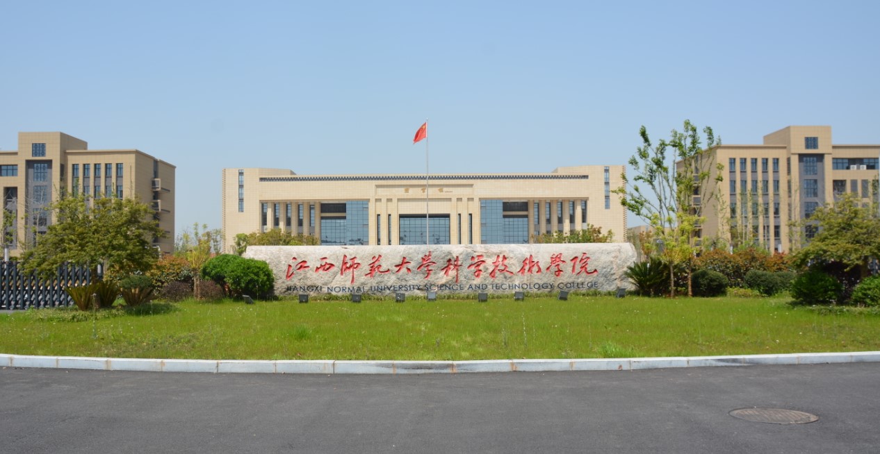
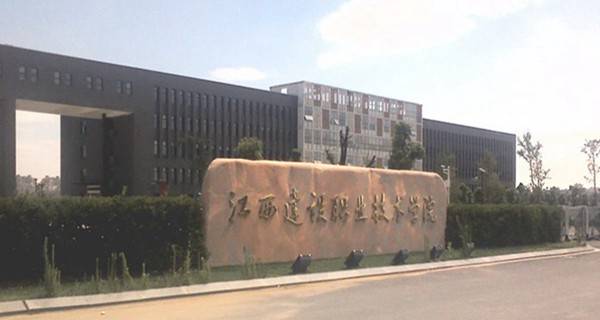
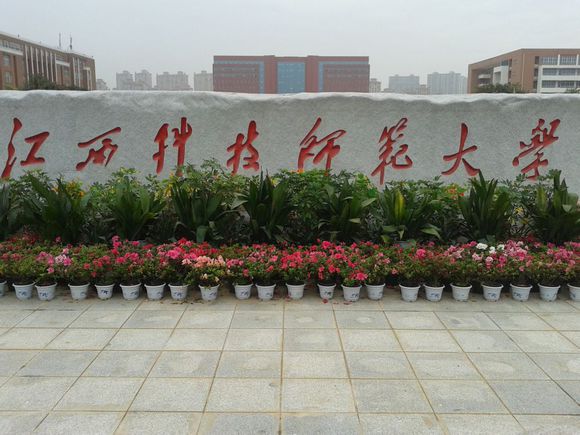
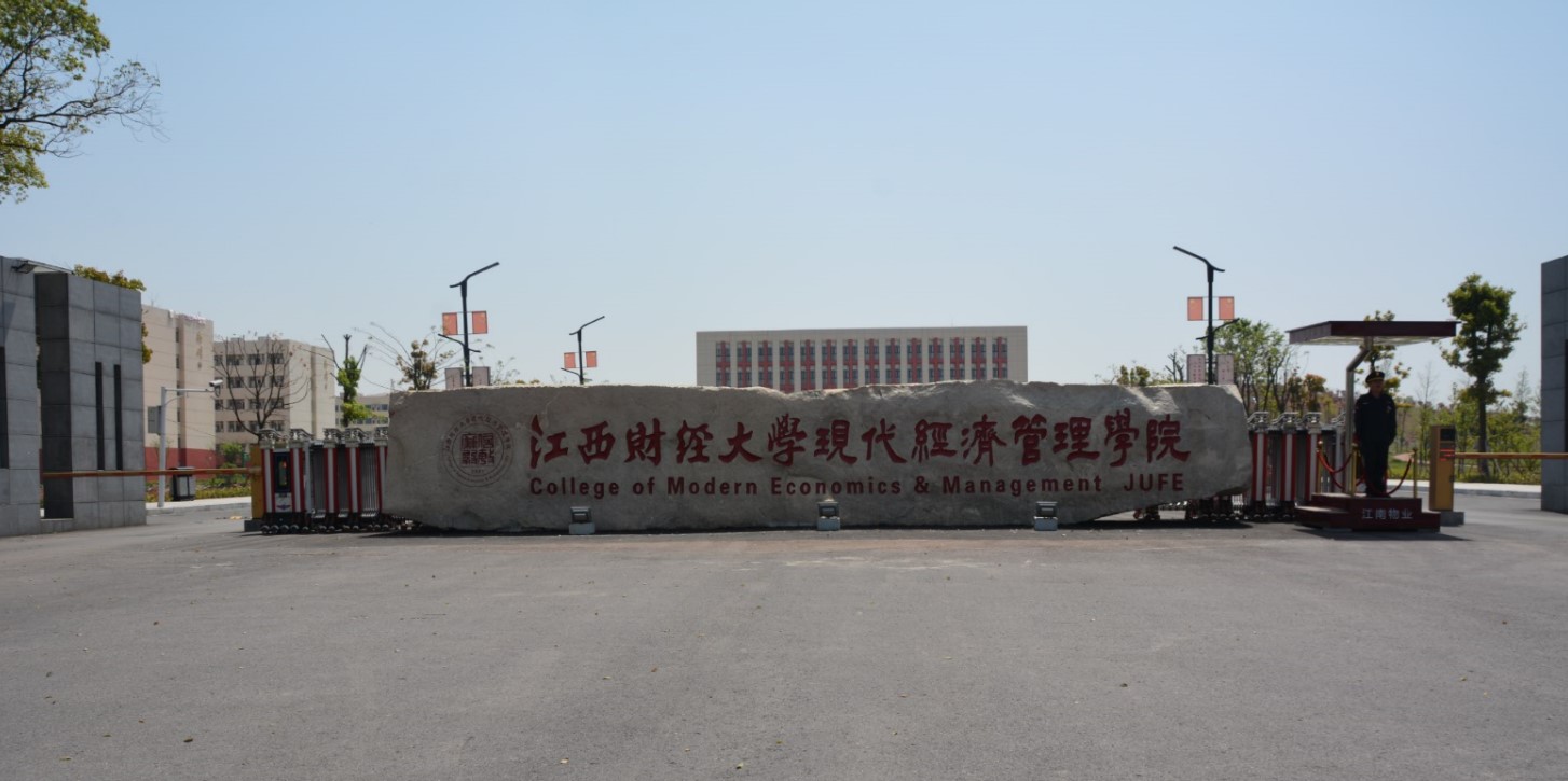
Volksamp Logo Banner


      WELCOME TO VOLKSAMP


The design objective was to arrive at a not too complex unit that nevertheless offered excellent performance, was fairly simple to build and could be reproduced relatively easily. The result is a straightforward amplifier without any unnecessary gimmicks.

A bipolar transistor may be considered a current-amplifying device that enables a (relatively) large current to be controlled by a much smaller one. A field-effect transistor (FET) behaves differently: it is a sort of variable resistance whose conduction is controlled by a voltage. It follows that the drives of these devices is quite different: an important consideration in the design of an output amplifier. A bipolar transistor needs a base current before it can function, whereas a FET can be driven almost without any energy. All it needs is a control voltage: the current it draws is negligible. When power FETs first came on to the market, many designers thought that they would simplify the design of output amplifiers beyond belief. That quickly proved to be not so, however, because power FETs have a fairly large capacitance between the gate and the drain/source channel (sometimes of the order of a few nanofarads). This means that at high audio frequencies the driver stages need to deliver fairly large transfer currents to keep the bandwidth sufficiently large.

It may well be asked what advantage(s) a FET offers. In a bipolar power transistor, it is difficult to combine high voltage, large current, and wide bandwidth, because its operation must remain within the Safe Operating Area-SOA. It is not enough to just look at the peak voltage and current in the relevant data sheet. By virtue of modern production techniques, FETs can be fabricated that can handle high voltages (100 V and more) and, in spite of their modest dimensions, large currents. It Is, therefore, much simpler to design an output amplifier with reasonable power output with power FETs than with power transistors. Of course, there are other requirements as well, such as slew rate and matching of complementary semiconductors...

The circuit

A symmetrical design has the advantage that it minimizes problems with distortion, particularly that associated with even harmonics. Therefore, the input stages consist of two differential amplifiers, T1-T2 and T3-T4. These use discrete transistors, not expensive dual devices, to keep the cost down. Performance is excellent, particularly if the transistors arc matched.

A differential amplifier is one of the best means of combining two electrical signals: here, the input signal and the feedback signal. The amplification of the stage is determined mainly by the ratio of the collector and emitter resistances (in the case of T1-T2 these are R9, R10, R11 and R12). These form a sort of local feedback: limiting the amplification reduces the distortion.

Two RC networks (R3-C3 and R4-C4) limit the bandwidth of the differential amplifiers and these determine, to a degree, the open-loop bandwidth of the entire amplifier (which is 6.5 kHz).

The d.c. operating point of the differential amplifiers is provided by two current sources. Transistor T6, in conjunction with R18 and D2, provides a constant current of about 2 mA for T1-T2. Transistor T5, with R17 and D1, provides a similar current for T3-T4. The combination of a transistor and an LED creates a current source that is largely independent of temperature, since the temperature coefficients of the led and the transistor are virtually the same. It is, however, necessary that these two components are thermally coupled (or nearly so) and they are, therefore, located side by side on the printed-circuit board.

In the input stage, C1 is followed by a low-pass section, R1-C2, which limits the bandwidth of the input to a value that the amplifier can handle. Resistor R2 is the base resistor of T1 and T3. So far, this is all pretty normal. Network P1-R7-R8 is somewhat out of the ordinary, however. It forms an offset control to adjust the direct voltage at the output of the amplifier to zero. Such a control is normally found after the input stage. The advantage of putting it before that stage is that the inputs of the differential amplifiers are exactly at earth potential, which means that the noise contribution of their base resistors is negligible.

The signals at the collectors of T1 and T3 are fed to pre-drivers T8 and T9. Between these transistors is a 'variable zener' formed by T7 which, in conjunction with P2, serves to set the quiescent current of the output FETS.

The output of the pre-drivers is applied to T10 (BD139) and T11 (BD140), which drive HEXFETs T12 (IRF9540) and T13 (IRF540). This power section has local feedback (R30-R31).

The design of T10-T13 is a kind of compound output stage, since the drain of the power FETs is connected to the output terminal. Note that T12 is a p-channel FET and T13 an n-channel type. Therefore, the stage provides current amplification as well as voltage amplification. The voltage amplification is limited to x3 by the local feedback resistors (R30-R31). Here again, this feedback serves to reduce the distortion. The overall feedback of the amplifier is provided by R5-R-C5.

Fuses are provided in the source lines of the HEXFETs. Power FETs have an inherent current limitation by virtue of their positive temperature coefficient: when the device gets hot, its drain-source resistance rises and this reduces the current through it. The fuses and this property provide adequate protection against brief short-circuits. Note that the HEXFETs used can handle peak currents of up to 75 A. Electrolytic capacitors C11 and C12 (10.000μF each and part of the power supply) are located close to the FETs, so that the heavy currents have only a short path to follow.

At the output is a Boucherot network, R32-R33-C10, that ensures an adequate load on the amplifier at high frequencies, since the impedance of the loudspeaker, because of its inductive character, is fairly high at high frequencies.

Inductor L1 limits any current peaks that may arise with capacitive loads.

The signal is finally applied to the loudspeaker, LS1, via relay contact Re1. The relay is not energized for a few seconds after the power is switched on to obviate any plops from the loudspeaker. Such plops are caused by brief variations in the direct supply voltage arising in the short period that the amplifier needs to reach its correct operating level.

The supply voltage for the relay is derived directly from the mains transformer via D3 and D4. This has the advantage that the relay is deactuated, by virtue of the low value of C13, immediately the supply voltage fails. The delay in energizing the relay is provided by T14 in conjunction with R36 and C14. It takes a few second before the potential across C14 has risen to a value at which T14 switches on. This darlington transistor requires a base voltage of not less than 1.2 V before it can conduct.

The power supply - see Fig. 2 - is traditional, apart from the resistors, R5-R8 in the power lines. These limit, to some degree, the very large peak charging currents to electrolytic capacitors C11 and C12. Moreover, together with these capacitors, they form a filter that prevents most spurious voltages from reaching the amplifier. Measurements on the prototype showed that this was particularly evident at frequencies below 500 Hz.